Enabling Ultrasensitive Measurements
EOI is a well-equipped small technical house whose mission is to enable our customers to produce advanced measurement products for their customers. As technology developers we find imaginative solutions to hard measurement problems in very many areas of optics, electronics, photonics, and mixed-technology systems, both for customers and for our own proprietary developments, as well as doing extensive expert witness work in optics and electronics cases.
We're also easy to work with. Send us an email and let's talk about your measurement.
-
Featured Product: LA-22 Low Noise Lab Amplifier
The LA-22 Low-Noise Laboratory Amplifier, 800 Hz–22 MHz, 1.1 nV / √Hz
One problem that comes up again and again in doing measurements is that we need the apparatus to be quieter than the thing we're measuring, ideally by at least a factor of two. Besides quiet, it should be wideband, have an accurately known gain that's flat with frequency, have a clean step response, and generally do its job while keeping itself out of the way. There's a wealth of detail in our app note AN-1 on photoreceiver testing.
read more…
-
"Super-Regenerative Receivers" by J. R. Whitehead
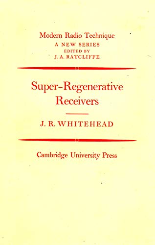
A quick plug for a little gem of a book that all fans of early radio should know about: "Super-Regenerative Receivers" by J. R. Whitehead (Cambridge University Press, 1950). It's part of the Modern Radio Techniques series, where a bunch of the technical movers and shakers document the advances that were made during the war, e.g. centimeter radar. This one is about the theory and practice of superregenerative radios. I learned a lot from it and had a lot of fun.
read more…
-
Temperature Control 1: Simple Control Theory
Temperature Control
The need to control temperature is everywhere, but getting it right is more difficult than one might expect. A domestic furnace controlled by a simple thermostat keeps a house comfortable in winter, but the inside air temperature swings irregularly over a range of a few degrees. That's fine for a house---you can have a New Year's party, with a bunch of people dissipating a hundred watts each, doors to hot ovens and the cold outside opening and closing, no worries whatsoever. The heating system keeps it comfortable.
read more…
Technical Hints & Usenet Discussions
I can often be found on the Usenet groups sci.electronics.design and sci.optics. (There's not a lot of activity at sci.optics these days, but there are still folks listening who can help. SED goes up and down, but is much more active.)
Those are great places to talk about optics and electronics, if you have a reasonably thick skin. There are a lot of smart people there who know their stuff and can help you. The clearer and more concise the question, the more helpful the answer, in general.
Usenet is generally unmoderated, which is a good thing in a busy group, because it keeps the discussion flowing. There are a few flamers, whom it's best to ignore.
(I used to hang out in alt.lasers as well, but the whole crowd moved to photonlexicon, which is more applications-oriented. The subreddit r/Optics has some knowledgeable folks too, if you like Reddit.)
Google Groups dropped Usenet support in February 2024, but it wasn't great for real use anyway. You'll need a mailer with decent filters, such as Thunderbird or Forte Agent.
Talk to you there!
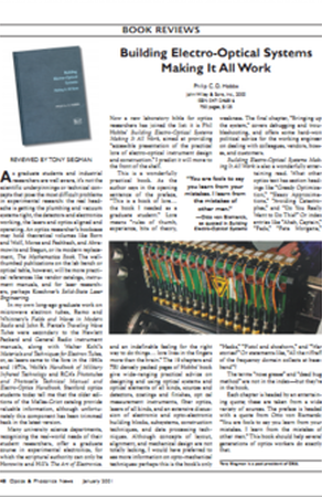
Building Electro-Optical Systems: Making it all Work

This book is an attempt to provide a systematic and accessible presentation of the practical lore of electro-optical instrument design and construction: in other words, it's the book I needed as a graduate student, but couldn't find.
It's intended in the first instance for use by oppressed graduate students in physics and electrical engineering, who have to get their apparatus working long enough to take some data before they can graduate. When they do, they’ll find that real-world design work has much the same harassed and overextended flavor, so in the second instance, it’s intended as a self-teaching guide and professional reference for working electro-optical designers.
For the third edition (February 2022), the book has been fully revised, and is almost a third again the size of the second edition, besides bringing in things learned in twelve years of consulting with EOI. The large format also made it possible to include a revised and expanded version of the thermal control chapter, which makes the printed book complete.
Now a new laboratory bible for optics researchers has joined the list; it is Phil Hobbs' Building Electro-Optical Systems: Making It All Work, aimed at providing "accessible presentation of the practical lore of electro-optical instrument design and construction." I predict it will move to the front of the shelf. This is a wonderfully practical book.... [It] is also a wonderfully entertaining read....
I like this guy's attitude. He points out how most scholars...never write about the troubles they had getting the apparatus to work right, or the changes they had to make to get valid data. Mr. Hobbs talks about exactly that. Good man. ...[I]f you work in this field, you ought to buy this book. If you don't work in this field, then you should still read it.
Look Inside
Table of Contents and Preface
Look Inside at Amazon
Chapter 20: Thermal Control
Chapter 20 didn't make it into the printed book due to length.Appendix: 100 Good Books
Recommended ReadingChapter Problems
Chapter ProblemsPlace To Buy
Officially: Wiley.com
-
Possibly Cheaper Sources: Barnes & Noble , Amazon.com , Amazon.ca , Amazon.co.uk , eCampus , or Metasearch at Bookfinder .
Consulting Services
I got started in consulting during my 20 years as a Research Staff Member at IBM T. J. Watson Research Center. I began in the Manufacturing Research department, building special instruments for unique manufacturing problems for which commercial solutions did not exist, such as scanned-probe and solid-immersion microscopy, and in-chamber particle detection. I also did a fair amount of firefighting, retrofitting semiconductor lithography equipment for new capabilities, and helping fix problems that were causing immediate revenue loss in manufacturing. Later I developed new classes of computer input device, advanced scanning technology, and a new class of photonic detector and switch for optical interconnection, based on metal-insulator-metal tunnel junctions.
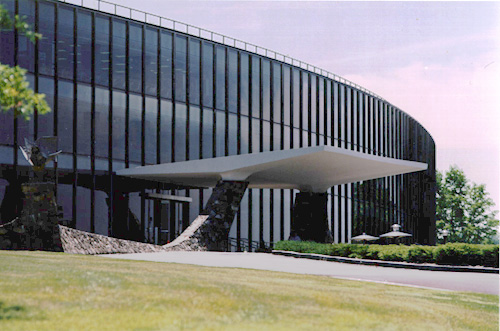
Front of Watson Research
The clear practical emphasis has never left me. One of the reasons that I wrote three editions of Building Electro-Optical Systems was to help people to build better products and apparatus while staying out of all the potholes in the road, and that's why I love consulting as well.
I do design consultation, expert witness work (testifying and consulting in patent and trade secret cases), contract design engineering, debug, and system bring-up tasks, as well as training in ultrasensitive detection methods and front end design. I hold 43 US patents and several foreign ones, and am thoroughly familiar with the patent process, both in prosecution (i.e. obtaining a patent) and litigation. Some of my earlier research and development projects appear below, and there's also a list of recent projects for clients.
I'm expert in the design, debug, and refinement of electrooptical and mixed-technology systems. I'm also a leading designer of ultrasensitive optoelectronics and other low noise analog circuitry. Many of my designs have improved the state of the art by orders of magnitude in performance, in cost, or both (see below). I've done groundbreaking work in thermal infrared imaging, in situ particle detection, computer input devices, simulation software, spectroscopy, atomic and magnetic force microscopy, solid immersion microscopy, heterodyne interferometry, trace metal detection, photolithography, laser scanning, plasmonics, and silicon photonics. I also have expertise in downhole instruments (especially stabilized lasers), disk drives, inspection systems, and semiconductor processing. There's more detail in my resume, as well as on the patents page, the recent work page and in the papers linked below.
On the design side, our customers to date are a mix of start-ups and larger companies, including some of the largest companies in the electronics, defense, oil-field services, and semiconductor equipment industries. We've worked as subcontractor or consultant on four defense contracts, for DARPA, the Office of Naval Research, and the Army. Our recent work page has some more details, but of course NDAs and other contractual obligations limit how much we can say about most of them. We're also introducing electro-optical instruments in cooperation with Highland Technology, a cutting-edge instruments company in California. On the intellectual property side, I'm a testifying expert witness in both patent infringement and trade secret misappropriation cases, with experience doing depositions, declarations, and expert reports, in both claim construction through validity or invalidity and infringement or noninfringement.
EOI is well-equipped for design, prototyping, and testing of optical, electronic, and mixed-technology systems of many kinds. If you have a tough technical problem and need the right solution fast, give me a buzz at the lab, 914-236-3005 (9-6 Eastern time, preferably). As always, the first hour or two is free, so if you'd like to discuss your application, you're invited to call, e-mail, or tell a colleague. I'm always interested to hear what folks are working on.
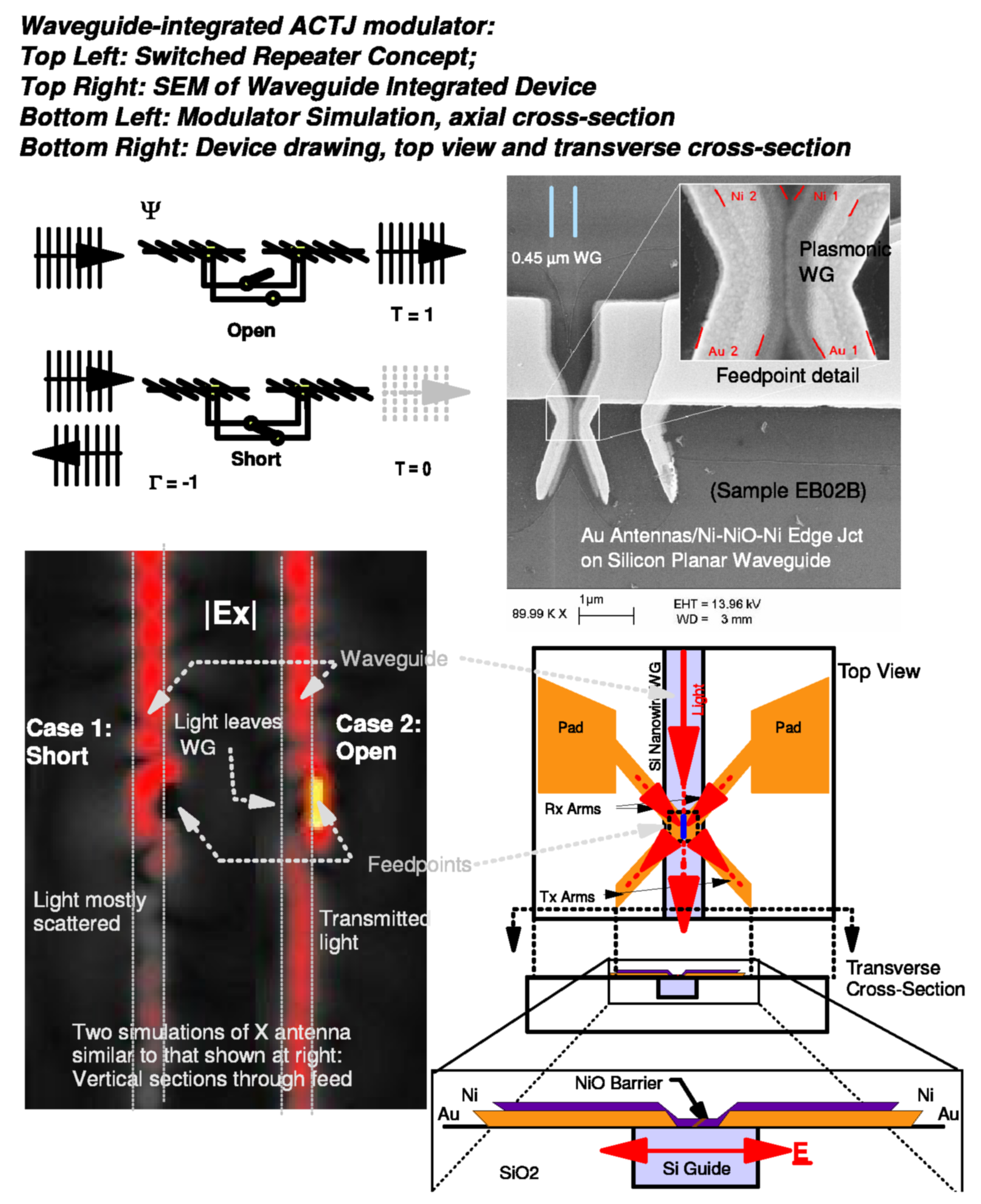
Antenna-Coupled Tunnel Junctions for Optical Interconnection
My silicon photonics work at IBM centred on the idea of integrating submicron silicon optical waveguides with metal plasmonic antennas and metal-insulator-metal (MIM) tunnel junctions, to build optical detectors and modulators in the 1.55 μm region.
They use a novel plasmonic travelling-wave structure to eliminate the effects of capacitance at optical frequencies—it's the fat metal bit in the middle of the X-shaped antenna arms, shown in the figure at right.
The attraction of this method is that it potentially eliminates the usual drawbacks of silicon photonic switching devices: narrow optical bandwidth, extreme temperature sensitivity, and high drive power. We estimated that it could reach drive power levels of less than 40 microwatts per Gb/s (40 fJ/bit), due to its low voltage swing (100 mV) and sub-femtofarad capacitance.
This is the project that POEMS was written for. We demonstrated the first waveguide-integrated ACTJ detectors, which have achieved a 40-fold increase in both response and sensitivity over any previous ACTJ detector.
We built all our own waveguide wafers as well as the ACTJ devices on top. The details of the junctions and fabrication procedures are here. Since beginning of my consulting business, I've done a couple of projects on these devices. One was with an aerospace client, for use as infrared pixels, and the other with a lidar startup. I expect more uses to develop, but probably not as an imager—we found that the rather low shunt resistance of these devices makes them quite insensitive at low light levels.
POEMS: Programmable Optimizing Electromagnetic Simulator
There are a variety of EM simulation schemes in wide use, with different strengths and weaknesses. For free-space antennas at radio frequency, where dielectrics are simple and metals are excellent conductors, integral equation schemes such as the method of moments (MoM) win. At optical frequencies, particularly when metal is involved, partial differential equation methods are generally better. The two most common PDE schemes are finite element method (FEM) and finite difference, time domain (FDTD). The antenna-coupled tunnel junction work required simulations with very fine resolution (1 nm) in some places, to represent plasmons and metal surface discontinuities, and a very large simulation domain, at least 5 μm square by 20 μm long. This requires multiprocessor capability and subgridding, i.e. different places in the simulation domain having different cell sizes. Subgridding is a natural strength of FE, but presents a challenge in FDTD, which naturally likes uniform cubical grids. On the other hand, mesh generation can be very time consuming, and FEM doesn't clusterize as well as FDTD and is much harder to get correct.
Lens design programs and circuit simulators have optimization capability—given a decent starting point (which may be hard to find sometimes), they will automatically adjust the lens prescriptions or circuit constants to achieve best performance by some criterion set by the user.
POEMS is a very capable FDTD simulator that brings this optimizing capability to the full EM world. I've mostly been using it to design waveguide-coupled antennas, but it's good for many sorts of EM problems. The current version uses either my own clusterized FDTD code, or (for verification) the well-tested but very much slower Berkeley TEMPEST 6.0 FDTD code for its number crunching engine. Here's the manual
The POEMS clusterized FDTD engine is currently working on EOI's AMD servers in an ad-hoc cluster with about 1 TFLOPS. Besides the original ACTJ devices, we've used it to design fluorescence-detection biochips for DNA sequencing, IR imaging, and coherent lidar. Its previous incarnations ran on a 24-way SMP and a 7-node, 14-processor Opteron cluster.
Scaling performance on these small SMPs and clusters is excellent, with less than 30% deviation from linear scaling of the single-machine version. In multicore boxes, this is due to some issues with the Linux thread scheduler, and in clusters, there is also communications latency over even the fastest Ethernet connections. The reason my code is so fast is that it precomputes a strategy, which allows a very clean inner loop iterating over a list of 1-D arrays of identical voxels, whereas, like most FDTD codes, TEMPEST has a big switch statement inside triply nested loops to decide what to do at each voxel on each iteration. That makes optimization and caching muc more difficult.
For more details, here's the manual. Send me an e-mail if you have a problem that might benefit from POEMS.
Laser Noise Cancellers
Laser noise is very often the primary limiting factor in making high-accuracy optical intensity measurements. There are ways of making your laser quieter, but they won't get to the shot noise level. On the other hand, what we actually measure is the photocurrent, not the laser power, and that we can improve.
Laser Noise Cancellers are extremely powerful devices that allow us to make shot-noise limited measurements at baseband, even with very noisy lasers. With zero adjustments, they will reliably suppress the effects of laser residual intensity noise (RIN) by 55 or 60 dB from dc to several megahertz, and with a bit of (optical) tweaking, will do 70 dB or more at low frequency, which is where it's most needed (see the picture above, which shows > 70 dB suppression of noise intermodulation). There's a New Focus app note which surveys applications of noise cancellers.
The laser noise canceller has two operating modes, linear and log-ratio. The linear mode produces a replica of the photocurrent minus the noise. The log ratio mode also suppresses the intermodulation of the laser noise with the signal, allowing (for example) tunable diode laser spectroscopy to achieve 1-ppm sensitivities even when the laser power is varying by >30% over a scan line, as shown here.
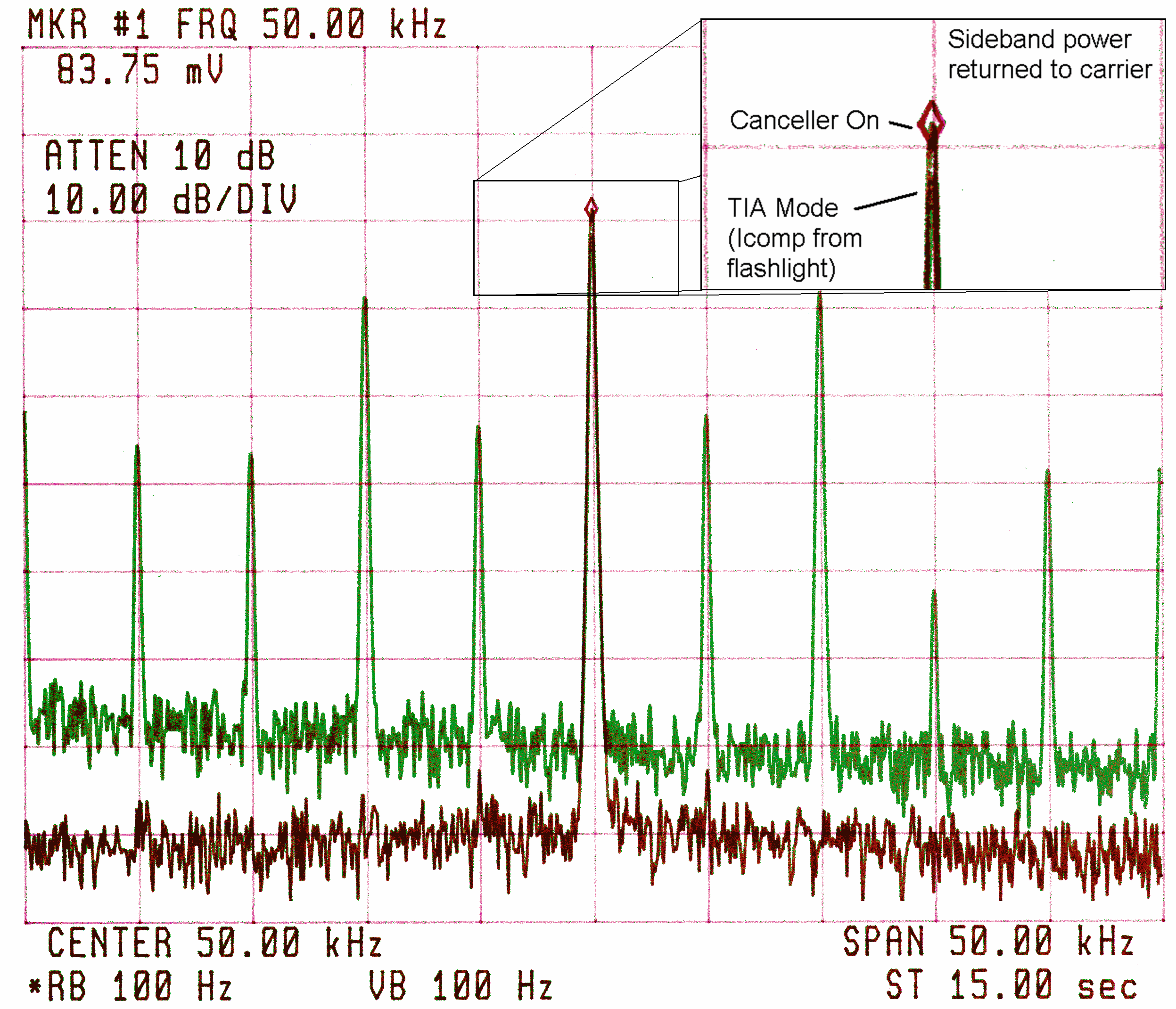
Laser noise canceller performance, showing the intermodulation suppression action of the log ratio output. The desired signal is the 50 kHz central peak, but the laser has additional unwanted 5 kHz AM, which puts intermodulation sidebands on the desired signal.
Upper trace: Single-beam TIA mode (comparison beam replaced with constant current to show actual photocurrent spectrum);
Lower trace: Normal dual-beam ratiometric operation (comparison beam unblocked), showing spurious intermod suppressed by 60-70 dB.
Note that the sideband energy has been returned to the main peak, as expected.
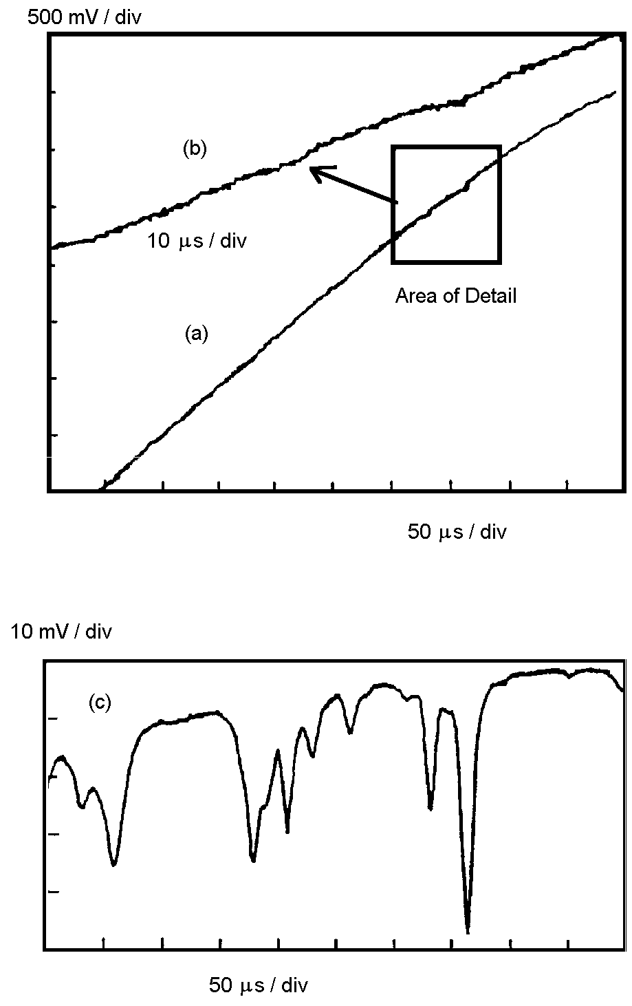
Elimination of sloping baseline and peak-height variations. Here's one way the previous figure translates into real measurement benefits.
Top: Raw detected photocurrent, comparison beam blocked. Spectral features are barely detectable bumps on a huge nonlinear sloping baseline, even in the detail view.
Bottom: the spectral region of the detail (about 0.5 cm-1) with the log ratio output of the noise canceller. The noise intermodulation suppression of 70 dB or thereabouts makes the peak heights independent of the laser power variations, so the lower trace gives sample absorbance directly, at a sensitivity better than 10-6.
Publications
Ultrasensitive Laser Measurements Without Tears
The definitive summary of my early work on noise cancellers: Six easily-constructed circuits that can improve the SNR of bright-field laser measurements by as much as 70 dB at low frequency and 40 dB out to 10 MHz. Bright field measurements at the shot noise limit become much easier.
The circuits are simple to construct (as simple as 1 dual op amp and 3 jellybean transistors), so anyone who can handle a soldering iron can improve the quality of his laser measurements enormously. Detailed applications advice is provided.
A word of caution: these circuits are easy to build but fairly hard to improve. Even if you want some custom tweaks, build the circuit as described, test it, and then change it around. You will have to add the usual 0.1 μF bypass caps on the supplies, and replace the discontinued Analog Devices MAT04 matched quad with the MAT14, but no other changes are necessary. Use ground plane construction, e.g. dead bug on a piece of Cu-clad FR4, or perf board style on a Vector 8007 protoboard, use nice quiet power supplies and/or capacitance multipliers, and don't put the photodiodes on cables. Bring the beams to them, instead.
Other important points: put a polarizer right at the laser to eliminate the spontaneous emission in the orthogonal polarization state, since it doesn't split the same way as the laser light, causing imbalance in the subtraction; and whatever you do, don't vignette the beams after splitting them.
(Applied Optics 36, 4 pp 903-920 [1 February 1997]).
In my consulting work, I've extended laser noise canceller technology out to higher speeds (10-100 MHz) and wider photocurrent ranges.
Double beam laser absorption spectroscopy: shot-noise limited performance at baseband with a novel electronic noise canceller
(Kurt L. Haller&Philip C. D. Hobbs)
Use of the log ratio version of the laser noise canceller to achieve 10-6 absorption sensitivity in current-tunable diode laser spectroscopy, even when the laser power changes by 30% over a scan. This is shown by the pictures at right. Using the well studied rovibrational spectrum of molecular iodine allowed us a simple demonstration system for a widely applicable technique, subsequently used in many instruments.
(Proc SPIE 1435, pp. 298-309 [1991])
Reaching the Shot Noise Limit for $10
Popular article on the laser noise canceller, from Optics&Photonics News, April 1991. An updated and somewhat chattier version of the SPIE paper below, with more discussion of applications. (Optics & Photonics News 2 4, pp. 17-23 [April 1991])
Shot Noise Limited Optical Measurements at Baseband with Noisy Lasers
First description of the laser noise canceller, including comparisons with heterodyne systems and use with helium-neon lasers showing mode beat suppression by >50 dB.
(Proc SPIE 1376, pp. 216-221 [1990])
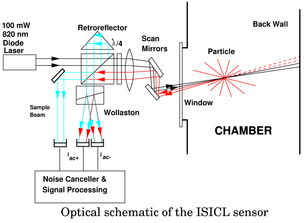
ISICL: In Situ Coherent Lidar for Submicron Particle Detection
Particles in plasma etch chambers are a major source of yield loss in semiconductor manufacturing. Particles condensing from the plasma or spalling out of films on the chamber walls are levitated in the edges of the plasma sheath for long periods, and then (too often) drop on the wafer when the plasma excitation is turned off.
Process control and tool utilization can both be improved by knowing what's happening inside the chamber while the process is going on—but how? The plasmas are usually too bright to look at, and there's only one (poor quality) window in the typical chamber, so an optical particle detector would have to work in backscatter, with a huge background.
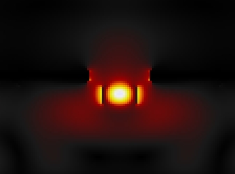
ISICL is capable of seeing and mapping individual particles of less than 0.2 μm diameter, as they float around in the plasma, a unique capability.
An interesting combination of homodyne interferometry, laser noise cancellation, and signal processing allows reliable operation at the shot noise limit in the face of a coherent background 106 times larger than the signal and an incoherent background 108 times larger.
The techniques I developed for ISICL have proven to be very widely applicable. My collaborators David Bomse and Daniel Kane at Mesa Photonics have had a DOE project for a receiver of a similar design in a spectroscopic sensor for nuclear nonproliferation monitoring, based on heterodyne detection of sunlight.
Even more recently, with a large industrial customer, I have been working on an advanced version of ISICL for detecting and mapping submicron particles moving at extremely high velocity. Calculations show that with only a watt of laser power, we should be able to see 0.15 μm particles moving at up to 3 km/s, i.e. Mach 9. I'll post more as this exciting opportunity develops.
ISICL: In Situ Coherent Lidar for Particle Detection in Semiconductor Processing Chambers
Detailed paper on the physics, design, and experimental results from the ISICL sensor.
(Applied Optics, 34(9), March 20, 1995)
Sensitivity and Sampling Rate of the ISICL Sensor
(Philip C. D. Hobbs & Marc A. Taubenblatt)
Calculation vs experiment for the photon budget, signal processing, and detection strategy of the ISICL sensor. Shows that a photon budget is worth following, even in a complicated instrument used in hostile conditions.
(Proc. SPIE 2909 1997 P11-20)
Heterodyne Confocal and Solid Immersion Microscopy
Optical phase is a wonderful thing—it can get you good topographical images of samples with no discernible amplitude contrast, for example, or allow you to disambiguate phase features from amplitude ones. My interest in phase-sensitive microscopes dates back to my graduate work—hence this paper. It gives design details and the theory of the heterodyne scanning laser microscope, including the point- and line-spread functions, plus a deconvolution method that can give resolution equivalent to an ordinary microscope working at λ0/2—ultraviolet resolution from a visible-light scope. Operating with a green Ar+2 laser (514.5 nm) and 0.9 NA, it attained a 10%-90% edge resolution of 90 nm.
This works because the interferometer makes it a confocal microscope, i.e. its amplitude point-spread function is the square of the illumination PSF. By the convolution theorem of Fourier transforms, that means that its bandwidth is twice as wide, i.e. ±2NA/λ. A bit of digital filtering turns the resulting nearly-triangular transfer function into something a bit more Gaussian-looking, which gives us a factor of 2 resolution improvement. Unlike the usual image processing ad-hockery, Fourier filtering makes absolutely no additional assumptions about the sample; the additional information comes from measuring both phase and amplitude, which is why you need an interferometer.
Solid Immersion Microscopy
This work was one of the first applications of modern signal processing to optical microscopy, and led to what may have been the first invention of solid immersion microscopy. After grad school, I moved to IBM Yorktown to work in the Manufacturing Research department. At that time, IBM produced about 25% of the world's semiconductors. More than that, though, IBM computers were all emitter-coupled logic (ECL), based on bipolar transistors, which were the fastest thing on the planet.
The big advantage of ECL was its very high transconductance—it could drive long wires at speeds double those of contemporary CMOS. The downsides were power consumption and complexity: a typical ECL recipe of the day had about 600 process steps, versus about 300 for CMOS, and the resulting chips consumed more than twice as much power. Before about 1992, that was a very good trade, and IBM's advanced bipolar logic devices gave rise to lots of fascinating measurement problems.
Sam Batchelder, Marc Taubenblatt, and I invented a silicon contact microscope in 1989, as a method for inspecting the bottoms of 16-Mb DRAM trench capacitors, which at the time were very difficult to etch cleanly. (The basic idea for a silicon contact lens was Sam's—he originally wanted to use an Amici sphere.) While this was prior to any publication by others on the subject, the contact or solid immersion microscope was also being developed in the laboratory of my Stanford Ph.D. advisor, Prof. Gordon Kino, at about the same time. They took the first solid-immersion pictures, while we were busy trying to design a manufacturing tool. (See S. M. Mansfield & G. S. Kino, Appl. Phys. Lett. 57, 24, pp 2615 - 2616 (1990).) (The same idea is called a numerical aperture increasing lens [NAIL] by other groups. Neither is a very good name, but we're stuck with one or the other—it's too bad that we can't just call it a contact lens, because that's what it is.)
Early Development
In 1989, we had an initial optical design performed by Prof. Roland Shack of the University of Arizona, which showed that the hoped-for high resolution could be obtained, at least in the ray model. Work continued on the real instrument, including studies of how to make good contact to the back surface of the silicon wafer. (Interestingly a much earlier, special-purpose contact microscope was developed by C. W. McCutchen of the University of Cambridge: Appl. Opt. 1, 3, pp 253-259 [May 1962].)
In early 1992 I took the first pictures at a numerical aperture (NA) of 2.5, shown above. These were made by optically contacting a steep silicon plano-convex lens to the polished back surface of an 8-inch wafer (so that the centre of the lens was nearly at the front surface), focusing a 1.319 μm YAG laser beam through it at an NA of 0.7 with a Mitutoyo long working distance microscope objective, and mechanically scanning the wafer+contact lens assembly using a piezo flexure stage. Detection used an unresolved pinhole in a standard Wilson confocal (Type 2) configuration, so that the spatial frequency bandwidth is ±2NA/λ (twice as wide as the illumination spatial frequency bandwidth).
Contact Microscopy
When a spherical beam crosses the concentric lens's surface, its angular width doesn't change, but the refractive index goes from 1.0 to 3.5, so the NA goes up from 0.7 to 2.5. (There's also a 3.5x linear magnification, so no free lunch is involved.) Although the Mitutoyo lens was reasonably well corrected at 1.319 μm, the coatings on its many elements were horribly mistuned, enough that its internal reflections dominated the returned signal and caused all sorts of nasty interference fringes. Fortunately, because of its long working distance, I could sneak a chopper wheel in between it and the hemisphere; lock-in detection then recovered the signal from the wafer and rejected the spurious reflections.
First Confocal Images at NA=2.5
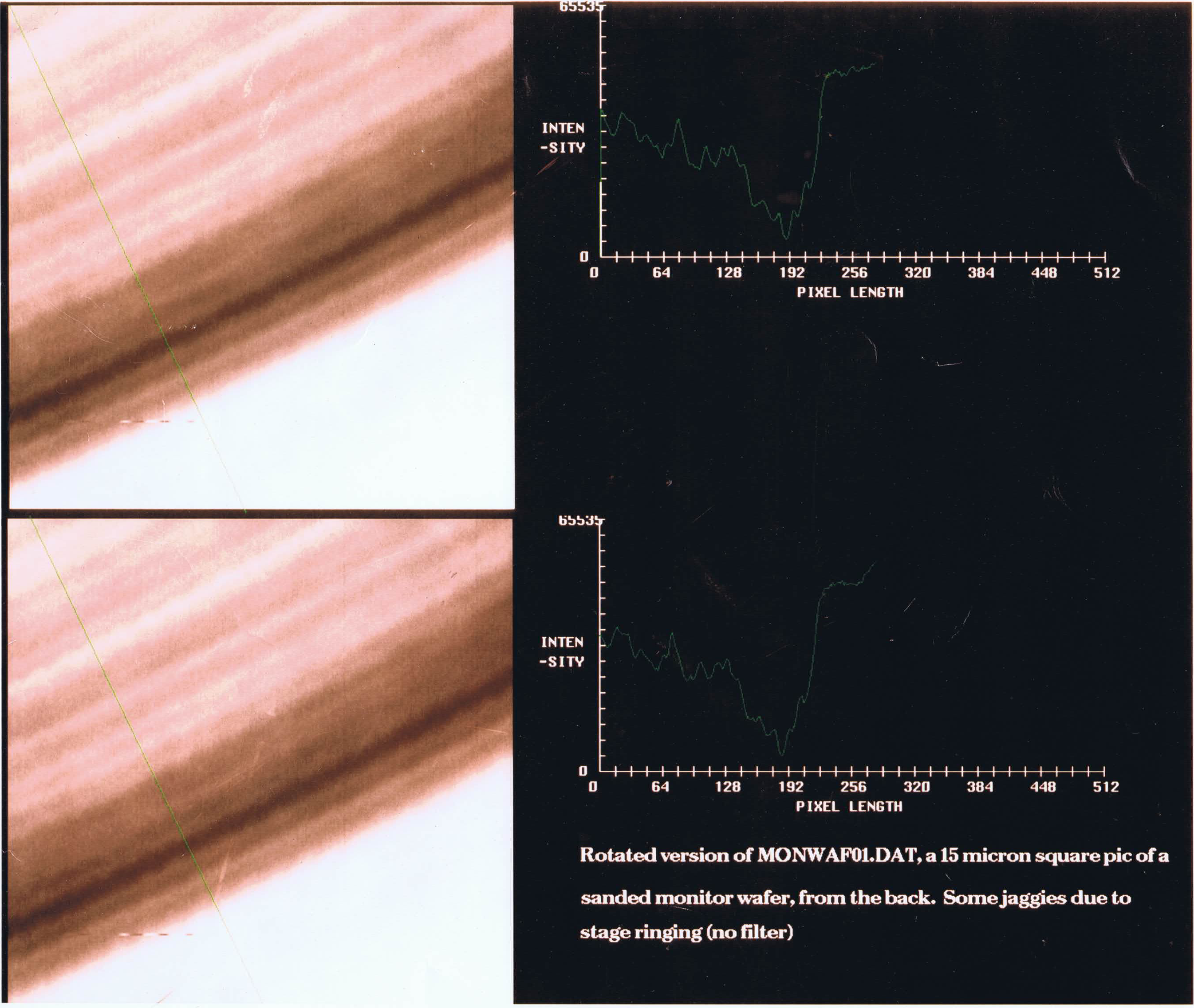
It turned out that we couldn't image real product wafers easily in our off-line lab, because there were fairly thick oxide and nitride films on the back of the wafer that made most of the light evanescent, as well as a lot of embedded particles which made the back surfaces too rough for good contact. Instead, I used a clean monitor wafer. A featureless flat surface isn't the most informative sample, of course, so I scratched the far side once, gently, with fine sandpaper. That produced a set of long fine grooves whose repeatable cross-section allows a good sanity check for a raster-scanned measurement; if the pattern repeats, it's probably real. It made the scenery rather boring, as you can see, but it's interesting as a technological demonstration.
The two frames have the same scan data, of a 15x15 μm area, but the two line scans are taken from positions about 5 μm apart along the groove, shown as the green lines on the images. There is repeatable detail with periodicities down to a bit below 0.30 μm (see e.g. the peak detail around pixel 128). That demonstrates a spatial frequency bandwidth of at least 4.4 cycles per wavelength, clearly more than the Type 1 limit of 2.5 cycles per wavelength at this NA. If it had been a phase sensitive design, I ought to have been able to use the deconvolution algorithm to achieve about 140-nm resolution at 10%-90%—equivalent to an NA of 5.0. (That's asking a lot of the objective, of course, but the heterodyne approach is pretty tolerant of minor imperfections.)
A Manufacturing Instrument
In 1Q 1990, we put out a request for bids, and by early 1992 we had a full-scale, 3.2 NA scanning heterodyne confocal instrument design completed, in cooperation with some very smart folks from Sira Ltd. of the UK: John Gilby, Dan Lobb, and Robert Renton. This design had a number of interesting features, including what may have been the first technological optical vortex. To allow easy navigation, we planned to make the instrument scan on a 50-nm air bearing. This was somewhat difficult, because at an NA above 1.0, the light in the air gap is evanescent. Not just a bit evanescent, either—at NA=3.2 the intensity falls off by 1/e2 in about 40 nm.
Tangential Polarization
Fortunately, we found a trick for this: it turns out that the falloff is very different in the two linear polarizations, with s polarization falling off n times more slowly than p. Thus we could avoid huge optical losses due to total internal reflection (TIR) at the air gap by using tangential polarization, i.e. the light incident on the air gap was always s-polarized. This was done by using a segmented half-wave plate shaped like an 8-petal daisy. Normally, surface reflections are reduced by using p-polarized light, as in polarized sunglasses, but with TIR, s-polarized is much better. We hoped to do measurements at an equivalent NA of 6.4, which would be pretty slick even today.
Optical Vortex and Daisy Waveplate
Along the way, we found that tangential polarization in the pupil leads to a very ugly focused spot with an amplitude null in the centre, i.e. an optical vortex. (We didn't think it was anything special at the time, except that it was spoiling our measurement.) We designed around this problem by using a circumferentially graded coating on the daisy wave plate to apply a one-cycle-per-revolution phase delay around the pupil circumference. That got rid of the vortex and improved the PSF a great deal: instead of a null, the field had a circularly polarized peak in the center, about as sharp as a normal linearly-polarized one, so by early 1992, everything looked good.
Unfortunately, as a result of IBM's near-death experience , both our customer and our budget went away later that year, so the system never got built. (I still have all the drawings.)
IBM had started making computers out of CMOS like everyone else, so Manufacturing Research was soon absorbed into another department with a software and services mission. For the next 15 years, I worked very happily on ultrasensitive instruments for semiconductor process control, computer input devices, low cost thermal imaging, advanced 3-D scanning, and especially silicon photonics, and never came back to contact microscopy. Fortunately others have made it a useful technique, though as far as I know, nobody has built one like ours.
Footprints: A $10 Thermal Infrared Imager
A low-resolution thermal camera with competitive sensitivity (0.13 K NETD) at very low cost. Easily built from scratch—it requires no special parts, except a screen-printed sheet of pyroelectric PVDF polymer (as used in automatic porch lights) and a moulded polyethylene Fresnel lens. This camera achieves a cost reduction of 2 orders of magnitude ($10 vs $1000) over the next cheapest, which is a 256-pixel PZT array from Irisys, while maintaining very good sensitivity. These are from a project called Footprints.
The design is simple: screen-printed carbon ink on a free-standing film of PVDF polymer, with a multiplexer made out of ordinary display LEDs with a few interesting optical and electronic hacks, as shown in these photos.
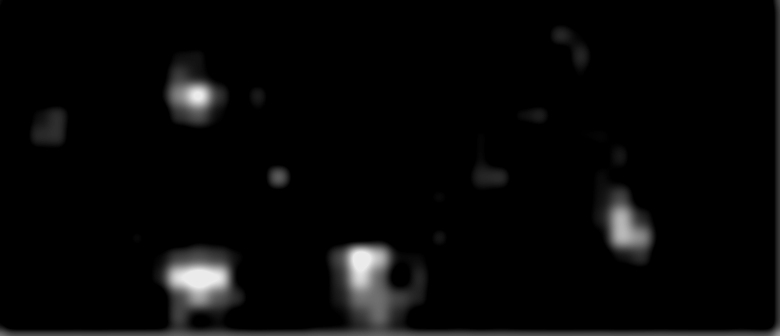
Mosaic image from 6 Footprints sensors, showing four people wandering underneath. Slightly smoothed to reduce the visual noise from all the little squares.
A fun war story from the September 2003 issue of Optics & Photonics News about the ups and downs of the Footprints project. (NB the war story link is free; the OPN one requires a log-in.)
The gory technical details: A $10 Thermal Infrared Imager
(Proc. SPIE 4563, 2001, p. 42-51).
We got a bunch of positive press reactions to this, including the NY Times and the Discovery Channel. We got a few negative ones too, but overall the fact that 30 cm pixel size makes everybody anonymous reassured people. (Nowadays, of course, video surveillance is ubiquitous, but back in 2000 privacy still existed.)
Movies of the sensor data
(NB: there aren't too many pixels, so you have to resize the video player to see much!)
IR video of customer demonstration, IBM Industry Solutions Laboratory, showing a bunch of folks standing around looking at this same (live) IR footage of themselves on monitors
2x3 mosaic, sensors 14 feet off the ground, suspended from a lighting boom at the Yorktown Stage
2x3 mosaic, sensors 10 feet off the ground, also at Yorktown Stage.
There are a few dead pixels, and the sensor in the bottom centre has a bad surface leakage problem, probably due to the very high humidity—data were taken during a thunderstorm.
Data were taken at 5 frames/s; the length scales are about 10 cm/pixel for the first, 30 cm/pixel for the second, one and 15 cm for the second.
(AVIs by courtesy of Sharathchandra Pankanti and Robert H. Wolfe.)
SiPM Module
Specifications
| 3dB Bandwidth | From DC–200 kHz to DC–300 MHz |
| Rise Time | 4ns (highest bandwidth configuration) |
| Gain Control Method | Gain settable by serial or analog voltage. Analog voltage control profile mimics behaviour of similar PMT modules. |
| Detector Type | Hammamatsu S13361/S13362 series or On Semi MicroFC series SiPm |
| Coupling | DC |
| Output Impedance | 50 Ω |
| Dynamic Range | All configurations support analog and photon counting |
| Power Requirements | +5V 100mA, -5V 10mA |
| Signal Output | SMA |
| Applications | Flow cytometry, Microplate readers, TOF Lidar |
In the last year or two we've been doing a lot of work aimed at replacing photomultiplier tubes (PMTs) in instruments, using avalanche photodiodes (APDs) and silicon photomultipliers (SiPMs). These devices are arrays of single-photon detectors, so they're also known as multi-pixel photon counters (MPPCs). Our main application areas include biomedical instruments such as flow cytometers and microplate readers, which have to measure low light levels very precisely but don't need the ultralow dark current of PMTs. (Follow-on articles will talk about our SiPM work in airborne lidar and SEM cathodoluminescence, as well as on improving the performance of actual PMTs.)
PMTs have been around since the 1930s, and remain the champs for the very lowest light levels. We love PMTs, but we have to admit that they're delicate and not that easy to use—they tend to be bulky, they need high voltage, and they need regular replacement. Most of all, PMTs are very expensive.
We've been working with several customers on developing products using Hammamatsu S13361/S13362 series and On Semi (formerly SensL) MicroFC series SiPMs. They have different strengths, but both series are excellent devices that have far better linearity in analog mode than we initially expected. (There's a fair amount of doom-and-gloom about that in the specialized technical literature.)
Our first product design uses the Hammamatsu units, and can go from counting single photons to working in analog in dim room lights, with just the twist of a knob. Subsequently we've had the opportunity to develop a couple of devices for time-of-flight lidar using the MicroFCs, which we developed from our existing IP. Recently we've been consulting on microplate and flow cytometry applications. All of these applications have in common that they're moving to the newer solid state option and away from traditional PMT-based designs.
These applications are challenging enough without having to develop the photodetection hardware. With so much customer interest, we've been focusing on developing a series of SiPM modules that act as drop-in replacements for traditional PMT modules, including all their nice features such as wide-range voltage-controlled gain, ±5 V input, and selectable bandwidths from DC–200 kHz to DC–200 MHz. Our existing designs are available on a flexible licensing model that generates considerable savings compared with either purchased PMT modules or internally-funded development, and gives you complete control over your supply chain.
Because these technologies are new, we can provide customized proof-of-concept (POC) demos showing how they work in your exact application. We've delivered prototypes and POCs in as little as one week at low cost, so you can make a real-world engineering evaluation without sacrificing a lot of budget or schedule.
For more information on our SiPM/MPPC designs, or help with your low-light measurements, send us an email or give us a call at +1 914 236 3005—we're interested in solving your detection and system problems.