Heterodyne Confocal and Solid Immersion Microscopy
Optical phase is a wonderful thing—it can get you good topographical images of samples with no discernible amplitude contrast, for example, or allow you to disambiguate phase features from amplitude ones. My interest in phase-sensitive microscopes dates back to my graduate work—hence this paper. It gives design details and the theory of the heterodyne scanning laser microscope, including the point- and line-spread functions, plus a deconvolution method that can give resolution equivalent to an ordinary microscope working at λ0/2—ultraviolet resolution from a visible-light scope. Operating with a green Ar+2 laser (514.5 nm) and 0.9 NA, it attained a 10%-90% edge resolution of 90 nm.
This works because the interferometer makes it a confocal microscope, i.e. its amplitude point-spread function is the square of the illumination PSF. By the convolution theorem of Fourier transforms, that means that its bandwidth is twice as wide, i.e. ±2NA/λ. A bit of digital filtering turns the resulting nearly-triangular transfer function into something a bit more Gaussian-looking, which gives us a factor of 2 resolution improvement. Unlike the usual image processing ad-hockery, Fourier filtering makes absolutely no additional assumptions about the sample; the additional information comes from measuring both phase and amplitude, which is why you need an interferometer.
Solid Immersion Microscopy
This work was one of the first applications of modern signal processing to optical microscopy, and led to what may have been the first invention of solid immersion microscopy. After grad school, I moved to IBM Yorktown to work in the Manufacturing Research department. At that time, IBM produced about 25% of the world's semiconductors. More than that, though, IBM computers were all emitter-coupled logic (ECL), based on bipolar transistors, which were the fastest thing on the planet.
The big advantage of ECL was its very high transconductance—it could drive long wires at speeds double those of contemporary CMOS. The downsides were power consumption and complexity: a typical ECL recipe of the day had about 600 process steps, versus about 300 for CMOS, and the resulting chips consumed more than twice as much power. Before about 1992, that was a very good trade, and IBM's advanced bipolar logic devices gave rise to lots of fascinating measurement problems.
Sam Batchelder, Marc Taubenblatt, and I invented a silicon contact microscope in 1989, as a method for inspecting the bottoms of 16-Mb DRAM trench capacitors, which at the time were very difficult to etch cleanly. (The basic idea for a silicon contact lens was Sam's—he originally wanted to use an Amici sphere.) While this was prior to any publication by others on the subject, the contact or solid immersion microscope was also being developed in the laboratory of my Stanford Ph.D. advisor, Prof. Gordon Kino, at about the same time. They took the first solid-immersion pictures, while we were busy trying to design a manufacturing tool. (See S. M. Mansfield & G. S. Kino, Appl. Phys. Lett. 57, 24, pp 2615 - 2616 (1990).) (The same idea is called a numerical aperture increasing lens [NAIL] by other groups. Neither is a very good name, but we're stuck with one or the other—it's too bad that we can't just call it a contact lens, because that's what it is.)
Early Development
In 1989, we had an initial optical design performed by Prof. Roland Shack of the University of Arizona, which showed that the hoped-for high resolution could be obtained, at least in the ray model. Work continued on the real instrument, including studies of how to make good contact to the back surface of the silicon wafer. (Interestingly a much earlier, special-purpose contact microscope was developed by C. W. McCutchen of the University of Cambridge: Appl. Opt. 1, 3, pp 253-259 [May 1962].)
In early 1992 I took the first pictures at a numerical aperture (NA) of 2.5, shown above. These were made by optically contacting a steep silicon plano-convex lens to the polished back surface of an 8-inch wafer (so that the centre of the lens was nearly at the front surface), focusing a 1.319 μm YAG laser beam through it at an NA of 0.7 with a Mitutoyo long working distance microscope objective, and mechanically scanning the wafer+contact lens assembly using a piezo flexure stage. Detection used an unresolved pinhole in a standard Wilson confocal (Type 2) configuration, so that the spatial frequency bandwidth is ±2NA/λ (twice as wide as the illumination spatial frequency bandwidth).
Contact Microscopy
When a spherical beam crosses the concentric lens's surface, its angular width doesn't change, but the refractive index goes from 1.0 to 3.5, so the NA goes up from 0.7 to 2.5. (There's also a 3.5x linear magnification, so no free lunch is involved.) Although the Mitutoyo lens was reasonably well corrected at 1.319 μm, the coatings on its many elements were horribly mistuned, enough that its internal reflections dominated the returned signal and caused all sorts of nasty interference fringes. Fortunately, because of its long working distance, I could sneak a chopper wheel in between it and the hemisphere; lock-in detection then recovered the signal from the wafer and rejected the spurious reflections.
First Confocal Images at NA=2.5
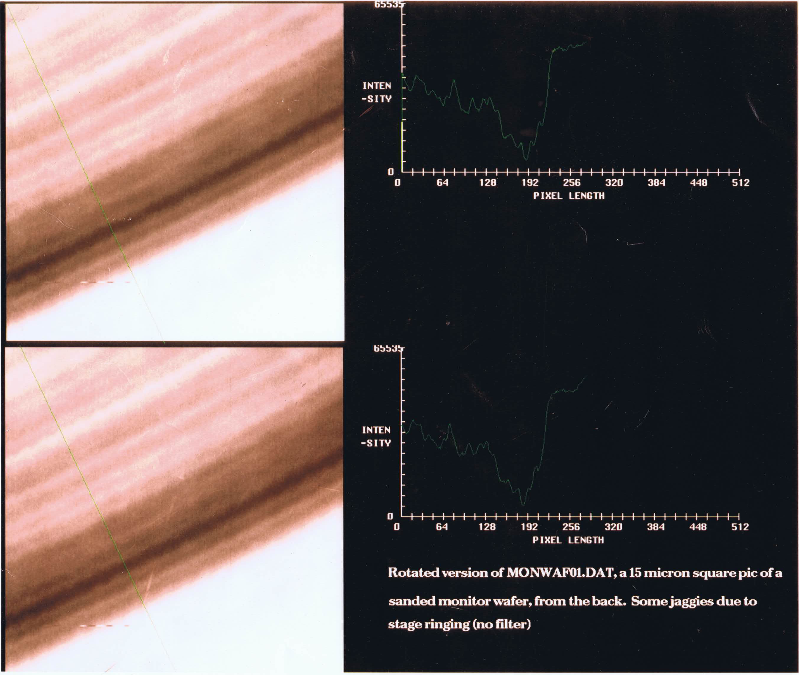
It turned out that we couldn't image real product wafers easily in our off-line lab, because there were fairly thick oxide and nitride films on the back of the wafer that made most of the light evanescent, as well as a lot of embedded particles which made the back surfaces too rough for good contact. Instead, I used a clean monitor wafer. A featureless flat surface isn't the most informative sample, of course, so I scratched the far side once, gently, with fine sandpaper. That produced a set of long fine grooves whose repeatable cross-section allows a good sanity check for a raster-scanned measurement; if the pattern repeats, it's probably real. It made the scenery rather boring, as you can see, but it's interesting as a technological demonstration.
The two frames have the same scan data, of a 15x15 μm area, but the two line scans are taken from positions about 5 μm apart along the groove, shown as the green lines on the images. There is repeatable detail with periodicities down to a bit below 0.30 μm (see e.g. the peak detail around pixel 128). That demonstrates a spatial frequency bandwidth of at least 4.4 cycles per wavelength, clearly more than the Type 1 limit of 2.5 cycles per wavelength at this NA. If it had been a phase sensitive design, I ought to have been able to use the deconvolution algorithm to achieve about 140-nm resolution at 10%-90%—equivalent to an NA of 5.0. (That's asking a lot of the objective, of course, but the heterodyne approach is pretty tolerant of minor imperfections.)
A Manufacturing Instrument
In 1Q 1990, we put out a request for bids, and by early 1992 we had a full-scale, 3.2 NA scanning heterodyne confocal instrument design completed, in cooperation with some very smart folks from Sira Ltd. of the UK: John Gilby, Dan Lobb, and Robert Renton. This design had a number of interesting features, including what may have been the first technological optical vortex. To allow easy navigation, we planned to make the instrument scan on a 50-nm air bearing. This was somewhat difficult, because at an NA above 1.0, the light in the air gap is evanescent. Not just a bit evanescent, either—at NA=3.2 the intensity falls off by 1/e2 in about 40 nm.
Tangential Polarization
Fortunately, we found a trick for this: it turns out that the falloff is very different in the two linear polarizations, with s polarization falling off n times more slowly than p. Thus we could avoid huge optical losses due to total internal reflection (TIR) at the air gap by using tangential polarization, i.e. the light incident on the air gap was always s-polarized. This was done by using a segmented half-wave plate shaped like an 8-petal daisy. Normally, surface reflections are reduced by using p-polarized light, as in polarized sunglasses, but with TIR, s-polarized is much better. We hoped to do measurements at an equivalent NA of 6.4, which would be pretty slick even today.
Optical Vortex and Daisy Waveplate
Along the way, we found that tangential polarization in the pupil leads to a very ugly focused spot with an amplitude null in the centre, i.e. an optical vortex. (We didn't think it was anything special at the time, except that it was spoiling our measurement.) We designed around this problem by using a circumferentially graded coating on the daisy wave plate to apply a one-cycle-per-revolution phase delay around the pupil circumference. That got rid of the vortex and improved the PSF a great deal: instead of a null, the field had a circularly polarized peak in the center, about as sharp as a normal linearly-polarized one, so by early 1992, everything looked good.
Unfortunately, as a result of IBM's near-death experience , both our customer and our budget went away later that year, so the system never got built. (I still have all the drawings.)
IBM had started making computers out of CMOS like everyone else, so Manufacturing Research was soon absorbed into another department with a software and services mission. For the next 15 years, I worked very happily on ultrasensitive instruments for semiconductor process control, computer input devices, low cost thermal imaging, advanced 3-D scanning, and especially silicon photonics, and never came back to contact microscopy. Fortunately others have made it a useful technique, though as far as I know, nobody has built one like ours.