Antenna-Coupled Tunnel Junctions for Optical Interconnection
My silicon photonics work at IBM centred on the idea of integrating submicron silicon optical waveguides with metal plasmonic antennas and metal-insulator-metal (MIM) tunnel junctions, to build optical detectors and modulators in the 1.55 μm region.
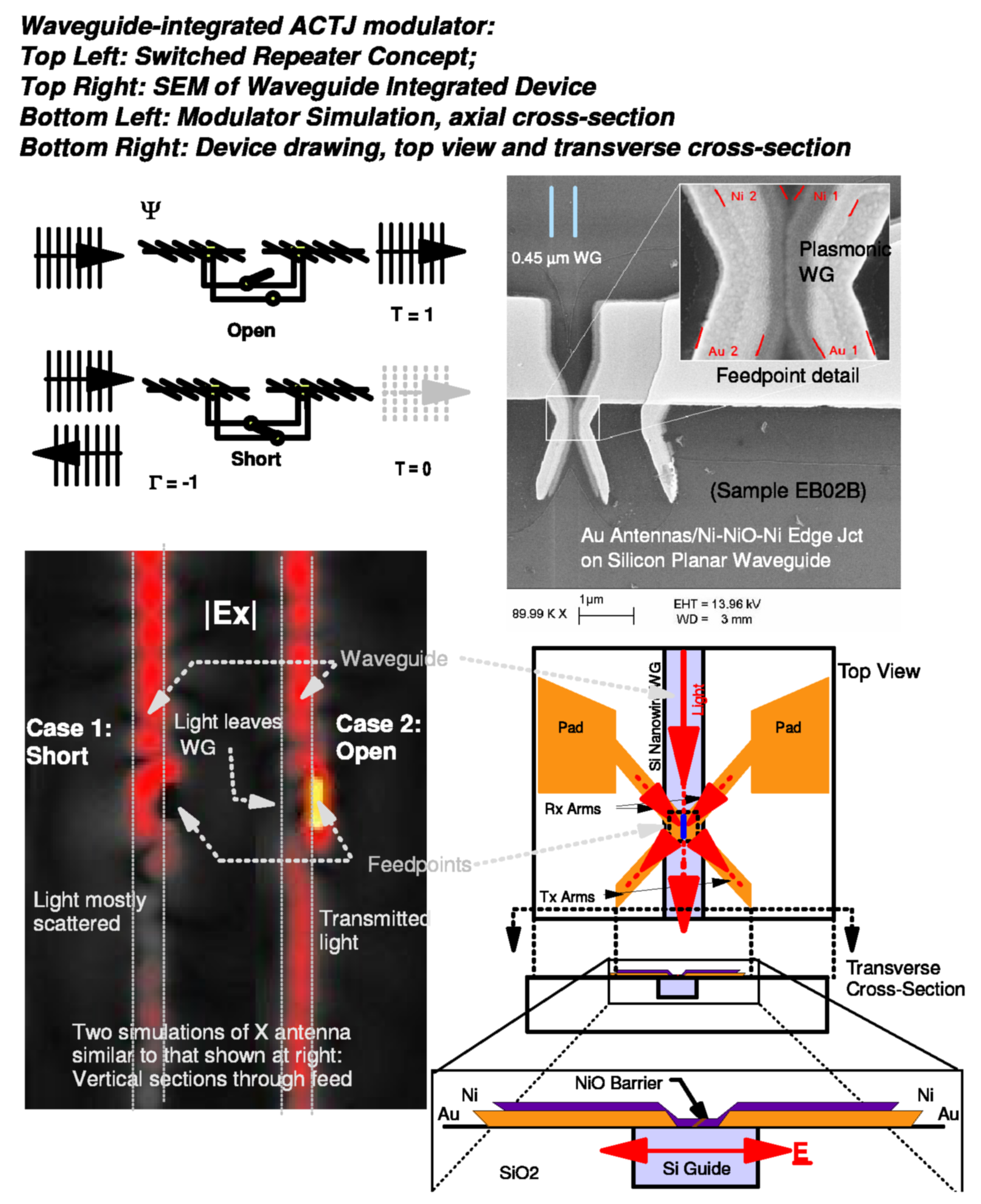
They use a novel plasmonic travelling-wave structure to eliminate the effects of capacitance at optical frequencies—it's the fat metal bit in the middle of the X-shaped antenna arms, shown in the figure at right.
The attraction of this method is that it potentially eliminates the usual drawbacks of silicon photonic switching devices: narrow optical bandwidth, extreme temperature sensitivity, and high drive power. We estimated that it could reach drive power levels of less than 40 microwatts per Gb/s (40 fJ/bit), due to its low voltage swing (100 mV) and sub-femtofarad capacitance.
This is the project that POEMS was written for. We demonstrated the first waveguide-integrated ACTJ detectors, which have achieved a 40-fold increase in both response and sensitivity over any previous ACTJ detector.
We built all our own waveguide wafers as well as the ACTJ devices on top. The details of the junctions and fabrication procedures are here. Since beginning of my consulting business, I've done a couple of projects on these devices. One was with an aerospace client, for use as infrared pixels, and the other with a lidar startup. I expect more uses to develop, but probably not as an imager—we found that the rather low shunt resistance of these devices makes them quite insensitive at low light levels.