Plate Reader for Water Quality Assay
Posted: 8 years, 10 months ago in Ultrasensitive Instrument Design
This is a research project with a small division of a very large manufacturer. It's a complete optical/electronic design to measure optical absorbance in a rapidly moving assay plate.
Shot-Noise Limited Sub-Nanoamp Photoreceiver for Spectroscopy
Posted: 8 years, 10 months ago in Ultrasensitive Instrument Design
This is a smaller job for a sensor manufacturer, interesting mostly for the size, weight, and power (SWaP) requirements. It has to be shot noise limited above 500 pA with a 1600 pF photodiode. (This is possible only because the bandwidth is relatively small.)
Doubling the Resolution of Solid Immersion Microscopes: Update
Posted: 8 years, 10 months ago in Ultrasensitive Instrument Design
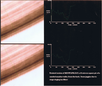
This is a very exciting development, in cooperation with a semiconductor equipment manufacturer. Back in 1989, my colleagues and I started working on a contact-lens microscope for looking into the interior of silicon chips through the back surface. In 1992 I took a picture (shown above) at a numerical aperture of 2.5, with resolution equivalent to NA 3.5 due to a confocal design.
The combination of this with my thesis work on doubling conventional microscope resolution via heterodyne interferometry and digital filtering was going to allow us to take images at an equivalent numerical aperture of 6.4. I never got to build the full scale system.
Now, over 20 years later, I finally get to do it for real. I'm designing and prototyping a microscope to work at NA 6.4, which will have resolution on the order of 15 nm (10%-90% rise). That's pretty cool stuff for a visible-light microscope, and if it works, it should give me bragging rights for a long, long time.
Cascode Enhancement pHEMT Photodiode Preamp
Posted: 8 years, 10 months ago in SED
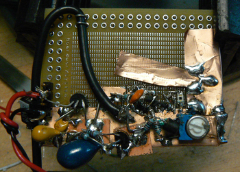
This is pretty small, because it has to be--those are microwave transistors, and will oscillate at the slightest provocation. The axial resistors and TO-92 parts are all for biasing---the actual amplifier is the part between the output coupling cap (the small orange thing in the middle) and the photodiode, which is the white square with the black middle at the right.
Transistor Tester for laser noise canceller
Posted: 8 years, 10 months ago in SED
As discussed in medium-gory detail in this paper, laser noise cancellers can let you do shot-noise limited measurements at baseband with lasers that are as much as 70 dB noisier than that.
Recent Posts
-
Featured Product: LA-22 Low Noise Lab Amplifier
-
 "Super-Regenerative Receivers" by J. R. Whitehead
 -
Temperature Control 1: Simple Control Theory
-
A High-Performance Time Domain Reflectometer
-
Product Announcement: QL03 Photoreceiver
Archive
2026
- January (1)
2025
2023
- May (1)
2021
- January (3)
2020
2018
2017
2015
2014
2013
2012
2011
Categories
- Design Support Consulting (8)
- Expert Witness Cases (15)
- New Technology (1)
- News (33)
- Products (4)
- SED (16)
- Sensitive Design (6)
- Ultrasensitive Instrument Design (27)
Tags
- photon budget (1)
- prototype (1)
- SEM (2)
- microscopy (1)
- microscope (1)
- product (1)
- noise (2)
- ultraquiet (1)
- thermoelectric cooler (1)
- Jim Thompson (1)
- analog-innovationscom (1)
- analog (2)
- ic design (1)
- scielectronicsdesign (1)
- website archive (1)
- MC4044 (1)
- MC1530 (1)
- SiPm (2)
- MPPC (2)
- PMT (1)
- Photomultiplier (2)
- frontend (1)
- module (2)
- hammamatsu (1)
- APD (2)
- SPAD (2)