What Photodetector Should I Use for Application 'X'?
We often get asked questions like, "How do I know what photodetector is best for (application X)?" For some values of X, it's pretty simple: if you've got milliwatts of visible light, use a silicon PIN photodiode and an ordinary transimpedance amp (TIA) made from an op amp or (for faster things) a packaged 50-ohm RF amplifier. It's usually easy to verify that you're in the shot noise limit---if your photocurrent drops more than 50 mV across its load impedance, you're there. (*)
That's a super useful rule, but you do have to watch out for another noise source: the eNC effect due to the shunt capacitance.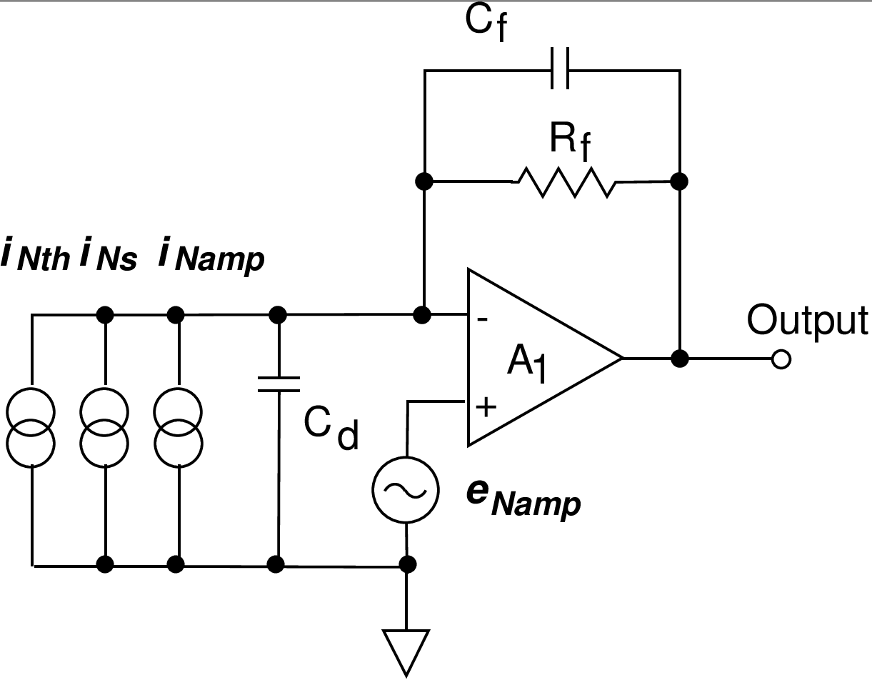
Figure 1: Simple noise model of a transimpedance amplifier. Thermal, shot, and amplifier current noise contributions add as currents, while the amplifier voltage noise gets multiplied by the noninverting gain of the stage.
Figure 1 shows a simple noise model of a transimpedance amp. There are three current noise sources: shot noise, thermal noise of RF, and the current noise of the amplifier. These all get dumped into the summing junction (the - input), so they appear in parallel in the model; that means they all get treated the same. The only noise source that isn't like that is the amplifier's input voltage noise. The amp is differential, so for analysis purposes we can put the source in either input. If we put it in the + input, it's obvious what happens: the - input tracks the + input, and the voltage noise gets multiplied by the absolute value of the noninverting voltage gain of the amplifier, called the noise gain. (The noise is a random variable so its phase doesn't mean anything.) It may be easier to see this by concentrating on the summing junction.
The photodiode is a high-Z current source, so it doesn't affect the DC noise gain. The shunt capacitance is
CS = Cd + Cin,
where Cd comes from the photodiode and Cin from the amplifier and the wiring. Because feedback makes the - input track the + input, eNamp appears across CS. At DC, CS doesn't do anything, so the noise gain is 1, but at AC, CS turns eNamp into a current noise
ieNC = 2 π f CS eNamp
that rises linearly with frequency. If the amp is fast enough, ieNC will dominate the shot noise when
2 π f eN CS > √ (2 e Iphoto).
This is even uglier than it looks, because although it only dominates at the high-frequency end, there's a lot more high end than low end---the total eNC noise in a bandwidth B is
INC = 2 π eN C √ ( B3 / 3 )
That B1.5 is startlingly worse than the B0.5 of the other noise sources, so as we widen the bandwidth, our SNR goes into the tank very fast. What to do?
We might try reducing Cd by increasing the reverse bias, or look for optical solutions, such as concentrating the light onto a smaller photodiode with less capacitance. Once we run out of options there, we may consider using a detector with gain of its own: an avalanche photodiode (APD), photomultiplier tube (PMT), or one of the newer array-type devices, a multi-pixel photon counter (MPPC) or "silicon photomultiplier" (SiPM).
We love PMTs, because they have a combination of high gain, low noise, and predictable performance that is very hard to beat, but they are expensive and need maintenance, so here we'll concentrate on silicon solid state detectors.
Avalanche Photodiodes
When light hits a photodiode, an incident photon knocks an electron loose from a silicon atom, forming an electron/hole carrier pair. A diode run at high reverse bias has a very large electric field in the junction region. If there are carriers (electrons and holes) present, the E field accelerates them in opposite directions. The carriers get scattered randomly every now and again, which limits how fast they go. If the field is large enough, sometimes these scattering events ionize (knock loose) another electron, forming another carrier pair. The new carriers can knock more electrons loose, and so on and so on, forming a chain reaction or avalanche, until all reach the metal contacts. How big the avalanche gets depends on the size of the E field and the distances between the first event and the contacts. If the voltage gets high enough, the avalanche current just goes up and up, so that the poor diode melts unless the current is limited externally. (This is how most 'zener' diodes actually work.) At slightly lower voltages, the avalanche dies out on its own after some number of ionization events, so that one detected photon produces an average of M carrier pairs in the external circuit. Interestingly, different materials have very different behavior.
Say our photodiode has a junction 1 mm thick. If a detected photon produces a carrier pair right in the middle, the electron and the hole both have to cover 0.5 mm to reach the contact. If only electrons cause impact ionization (as is nearly true in silicon), the initial hole just drifts to the (negative-biased) anode. The electron may cause a cascade of M impact ionizations, but all those holes travel placidly to the anode, and all the electrons reach the cathode at about the same time, at which point the avalanche stops. If electrons and holes are equally likely to cause ionization, the avalanche bounces back and forth, and stops only stochastically, when the last carrier reaches a contact. In order for this to happen, the gain per carrier has to be kept low to avoid trashing the SNR. InGaAs APDs don't work well above M = 10, whereas silicon continues improving up to M = 20 to 50.
An APD is similar to a regular PIN diode, with an anode and a cathode. The difference is that except that it
(*) You can derive this yourself, using the formulas for the shot noise of the photocurrent and the Johnson noise of the load resistance, equating them, and solving for VL = Iphoto*RL = 2 kT/e (~51 mV at 300K) where as usual k is Boltzmann's constant, e is the charge on the electron, and T is the absolute temperature. A packaged 50-ohm amplifier can be considerably quieter than a 300 K resistor--some have noise temperatures in the 50-K range.