One problem that comes up again and again in doing measurements is that we need the apparatus to be quieter than the thing we’re measuring, ideally by at least a factor of two. Besides quiet, it should be wideband, have an accurately known gain that’s flat with frequency, have a clean step response, and generally do its job while keeping itself out of the way. There’s a wealth of detail in our app note AN-1
on photoreceiver testing.
One of the most enjoyable parts of electronics design is getting excellent performance with rock-bottom parts cost. The right circuit can produce exceptionally good speed, noise, and accuracy specs from very low-cost parts. A case in point was a project from December 2016: a time-domain reflectometer (TDR) for a liquid level sensing application in industry.
TDRs work by sending short pulses down a transmission line where they bounce off anything that disturbs their propagation. By measuring the time delay, you can tell how far down the line the disturbance is. It’s a bit like a one-dimensional radar, except that with TDR you can learn a lot more from the reflection than just its location. TDRs can find damaged optical fibres, waterlogged sections of coax cable, and many other things of that sort. This application used an air-dielectric coaxial probe built from two metal tubes sticking downwards into a tank, so that the first part of the probe had air as dielectric and the second part had liquid. The dielectric constant of a liquid is at least 2, whereas air’s is 1.0, so there’s a nice healthy impedance mismatch at the surface to reflect the pulse. This approach is very rugged and resistant to fouling (you can get all sorts of nameless crud in process water and diesel tanks, for instance).
In the last year or two we’ve been doing a lot of work aimed at replacing photomultiplier tubes (PMTs) in instruments, using avalanche photodiodes (APDs) and silicon photomultipliers (SiPMs). These devices are arrays of single-photon detectors, so they’re also known as multi-pixel photon counters (MPPCs). Our main application areas include biomedical instruments such as flow cytometers and microplate readers, which have to measure low light levels very precisely but don’t need the ultralow dark current of PMTs. (Follow-on articles will talk about our SiPM work in airborne lidar and SEM cathodoluminescence, as well as on improving the performance of actual PMTs.)
In Part 1, we discussed ways to get better measurements by improving the signal to noise ratio (SNR), and saw that although it was often a win to measure more slowly and use lowpass filters, going too far actually makes things worse, because of the way noise concentrates at low frequency. Here we introduce a more sophisticated approach that generally works better: the lock-in amplifier.
We were considering a typical baseband signal, one that goes from near DC to some much higher frequency. Audio is a typical example, with a bandwidth usually quoted as 20 Hz to 20 kHz. To escape the low frequency noise, we need to move our signal up in frequency, out of baseband. In lock-in detection we make the signal periodic in time at some carrier frequency fc chosen to be several times higher than the required bandwidth. This is generally pretty easy to do, as we’ll see, and doing so ensures that none of the signal we care about remains near DC. Our noise rejection filter now needs to be a narrow bandpass centered at fc, so as to reject both low-and high-frequency noise. We’ll also need some means of measuring the amplitude and phase of the AC signal. That’s more complicated, of course, but with this setup we can narrow the bandwidth as much as we like and still get the full SNR improvement. A lock-in amplifier is a device for making such narrow-band AC measurements conveniently. It’s basically a radio that measures the phase and amplitude of its input, so that we recover a lowpass-filtered version of the baseband modulation signal that we care about, with no 1/f noise pollution to worry about. At this point we need to geek out a little bit and talk about modulation, which is what we mean by moving the signal away from baseband.
In building an ultrasensitive instrument, we’re always fighting to improve our signal-to-noise ratio (SNR). The SNR is the ratio of signal power to noise power in the measurement bandwidth, and is limited by noise in the instrument itself and the noise of any background signals, such as the shot noise of the background light or the slight hiss of a microphone.
If the signal is weak, it will have proportionally more noise, so that the apparatus has to be designed to get rid of as much noise as possible. There are a number of ways to do this. The best is to get more signal or reduce the noise, for instance by increasing the laser power and using a laser noise canceller, but eventually we hit a practical limit. At that point, we’re left with several options, all of which boil down to filtering in one form or another.
A thermoelectric cooler is a solid-state device made from two alumina ceramic plates with an array of metallized pillars in between. The pillars are also ceramic–they’re made of alternating p-type and n-type bismuth telluride (Bi2Te) semiconductors, alloyed with antimony telluride (p-type) or bismuth selenide (n-type), and connected in series electrically. The Peltier effect makes them electric-powered solid state heat pumps. (Thermocouples work the other way round, via the Seebeck effect, but the physics is the same.)
At EOI, we’ve been building advanced instruments for a long time. One reason for our success is our large inventory of working designs, and another is the way we go about doing it. This post walks through a typical sort of development plan for a challenging customer requirement, in the form of a hypothetical email proposal outline for a fibre-coupled noninvasive glucose sensor similar to the one we did in 2013. (You can also read about a recent project that went a lot like this, except with a single prototype stage.)
In How We Work, we gave an overview of how we build instruments, from the initial feasibility calculation (or photon budget) to delivery of the first production units.
Each project is different, of course, but there are common themes. Here’s a description of these steps from our most recent one at this writing (late January 2020), which is a low-cost cathodoluminescence detection system for use in scanning electron microscopes (SEMs).
Photon Budget
Cathodoluminescence Principles
A SEM works by scanning a tightly-focused beam of high-energy electrons (1 keV - 30 keV) across a sample, and looking at the stuff that comes out. For ordinary imaging you usually look at backscattered and secondary electrons, but there are other modes. For instance, you can get a lot of information about the sample’s chemical composition by looking at the x-rays it emits. Most samples will also emit some amount of light, a process called cathodoluminescence .
Here at EOI we have three main kinds of project. One is our internal technology development projects. Some of these fail, mostly because they tend to be insanely hard, but the ones that pay off give us important new capabilities.
The second is research projects with customers, trying to push technological limits in fields such as biochip DNA sequencing, nanoantennas for infrared detection, ultrahigh resolution optical microscopy, hypersonic lidar, and (closer to home) infrared remote controls for consumer electronics. Those ones are a bit sporty, but succeed more often than not.
In cooperation with Flatfrog Laboratories AB, Lund, Sweden. This one was interesting mostly due to the requirement for high and stable performance at an absolute rock-bottom cost.
This was a seedling design study for a DARPA program that never got funded. It leveraged POEMS and my antenna-coupled tunnel junction devices, adding a couple of novel wrinkles: metal-insulator-metal varactors and parametric readout using a 10 GHz pump frequency. Hopefully there will be a chance to revisit this, because it was potentially a pretty sweet solution.
For a large Far Eastern consumer electronics manufacturer to use in virtual reality games. A greatly improved transimpedance amplifier got them a factor of 10 in range (30 m vs. 3 m) for about the same amount of power.
This was in collaboration with a start-up in New Mexico called Symphony Acoustics. Downhole measurements are notoriously difficult, and this one was no exception: building a laser that could achieve an Allan variance of 10-10 at 10,000 seconds, and do it 5000 feet down a 2-inch cased drillhole. Due to the casing thickness, the maximum outer diameter of the instrument package was 38 mm, including its own casing and two concentric zones of thermal control.
This was in cooperation with Mesa Photonics of Santa Fe NM. It’s part of a DOE program, an advanced deployable solar occultation spectrometer for detecting volatile plumes from clandestine uranium enrichment.
Their scheme uses a really cool technique: solar heterodyne detection. It’s a good illustration of the importance of a photon budget.
A follow-on to the single channel version. This one had to work at very much lower power, which required a new amplifier topology based on local feedback around a very low noise JFET. This was a very fruitful development, which has been used in a number of follow-on designs.
In cooperation with InView Technology. Compressive scanning is a scheme for doing image sensing with a single-element detector, without suffering the N2 speed penalty of raster scanning. It’s a sort of combination of scanning and image compression—you use a digital micromirror device (DMD) to multiply the image by a series of 1-bit digital basis functions, measure the resulting photocurrent, and then invert the transform to produce a compressed image. That’s not too useful in the visible, where image sensors are cheap commodity items, but in the UV and especially the shortwave IR (SWIR), image arrays are extremely expensive, so there’s a need for compressive scan cameras.
This one came from a a major industrial research laboratory: near shot noise limited detection of 1 nA currents in 100 MHz bandwidth. This was one that I wasn’t at all sure would work: it’s pretty sporty trying to detect a few dozen electrons at 100 MHz in a built-up circuit. (A 100-MHz lowpass has a time-domain response about 5 ns wide, and 1 nA in 5 ns is 31 electrons.) Obviously to get the highest available signal voltage, the input-node capacitance has to be absolutely the minimum possible: less than 1 pF.
This is for for a scanning surface potential measurement tool, used in contamination detection in semiconductors: 40 attocoulomb sensitivity in a 4 MHz bandwidth
This was a prototype of a transcutaneous (through-the-skin) sensor for blood glucose and blood alcohol.
Optical and optomechanical design, detection and control electronics and software, prototype construction: first spectra were taken 5/16/2013, and technology transfer to a contract engineering firm was essentially completed 6/14/2013.
Most notable was the schedule requirement: from a standing start, in less than 6 weeks’ work, I did a complete photon budget, designed and built all of the optics and electronics, wrote all the software, integrated and shipped the system. It worked great.
A bit of a departure from our usual fare: a low cost, high speed sensor for detecting blood spots in eggs using spectral differencing. I’m going to be doing the firmware as well as the optics and electronics, and this will be the first actual client work for our newly qualified PCB designer, Magdalen.
Competing devices use xenon flashtubes and very expensive photodiodes, but still need a lot of calibration and tweaking. That makes it a good candidate for our signature technique: A really careful photon budget followed by a design that actually reaches the theoretical optimum performance.
This is a research project with a small division of a very large manufacturer. It’s a complete optical/electronic design to measure optical absorbance in a rapidly moving assay plate.
This is a smaller job for a sensor manufacturer, interesting mostly for the size, weight, and power (SWaP) requirements. It has to be shot noise limited above 500 pA with a 1600 pF photodiode. (This is possible only because the bandwidth is relatively small.)
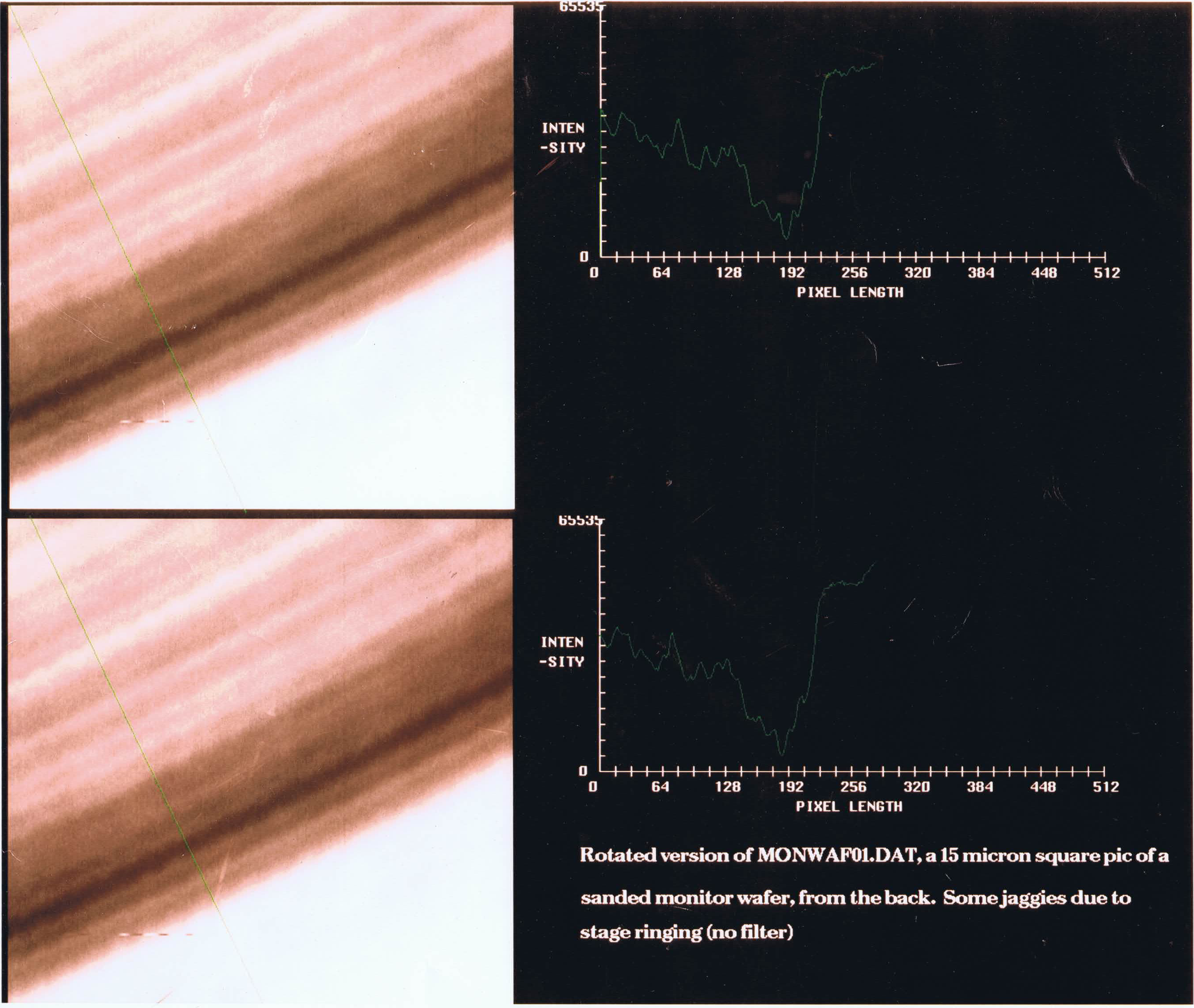
This is a very exciting development, in cooperation with a semiconductor equipment manufacturer. Back in 1989, my colleagues and I started working on a contact-lens microscope for looking into the interior of silicon chips through the back surface. In 1992 I took a picture (shown above) at a numerical aperture of 2.5, with resolution equivalent to NA 3.5 due to a confocal design.